Laser modules provide
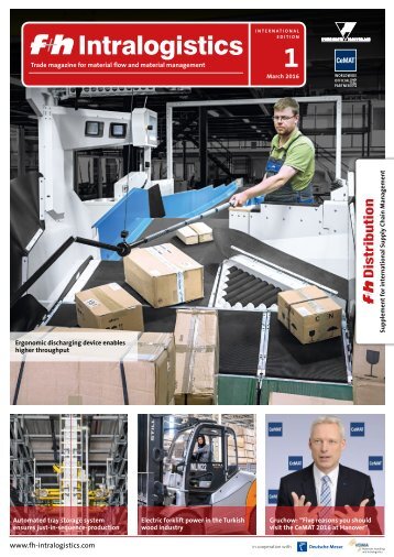
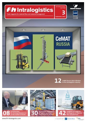
Laser modules provide improved efficiency for thin-film solar modules Manz AG is one of the world’s pioneers in photovoltaic engineering. In the realization of the largest order in the company’s history so far, Z-Laser laser modules play a decisive role in quality assurance and enable the production of solar modules with very high efficiency. With CIGSfab, Manz AG is the only supplier worldwide of a turnkey, fully integrated production line for the production of CIGS thin-film solar modules. “We are absolutely convinced that the future belongs to CIGS thin-film solar technology in photovoltaics,” emphasizes Bernd Sattler, Head of Vision & Metrology at Manz AG in Reutlingen. In January 2017, the company, which was founded in 1987, won the largest order by far in the company’s history with a volume of 263 million euros for this product: A joint venture of the Chinese Shanghai Electric Group Co., Ltd. and the Shenhua Group Co., Ltd. ordered a CIGSfab with a capacity of 306 MW and a CIGSlab, a research line with a capacity of 44 MW. Both factories are scheduled to start production in the summer of 2019. 50 times thinner than a human hair When checking the lines that are created in the first two structuring processes, laser modules ensure optimum illumination In a conventional crystalline solar module based on a high-purity silicon wafer, a large number of individual solar cells are soldered and mounted between a glass pane and a film. The individual wafers are up to 100 times thicker than the semiconductor layer CIGS (copper-indium-gallium-diselenide) on a thin-film module. This is vapor-deposited in a vacuum system, in just one process step, directly onto a glass pane. The use of expensive semiconductor material is correspondingly higher in crystalline technology. In addition, thin-film technology eliminates the labor-intensive and expensive multilevel process of the raw silicon, the wafer, the cell, and the module fabrication by direct application of the semiconductor to the glass substrate. The advantage according to Bernd Sattler: “The CIGS absorber layer has a thickness of only approx. 2 μm and is thus 40 to 50 times thinner than a human hair. The positive effects on the manufacturing costs due to the material savings and fewer process steps are obvious.” 01 In the P2 structuring machine, two laser processing heads are operated in parallel, which is why two Z-Laser illumination lasers are used on one unit AUTOMATION 18 WORLD OF INDUSTRIES 1/2019
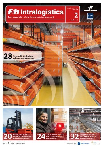
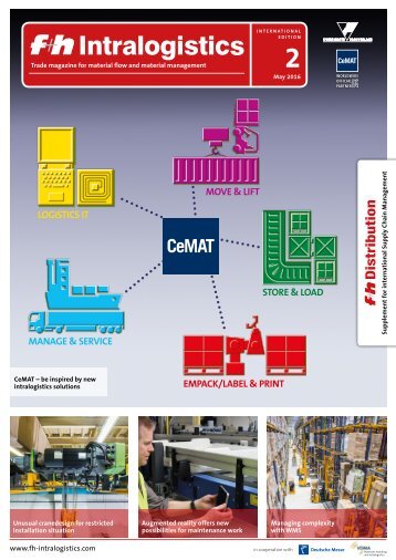
02 The CIGS absorber layer has a thickness of only about 2 microns and is thus about 40 to 50 times thinner than a human hair The manufacturing process of the 600 x 1 200 mm solar modules at Manz therefore requires the highest precision. Bernd Sattler describes the essential steps as follows: “The carrier material is coated and structured in several process steps. The entire area has to be divided into smaller cells, as the whole area generates a high current. By connecting these small cells in series, the voltage can be increased from about 0.6 V per cell to, for example, about 80 V per module. “This requires three separation steps, two of which are realized with one processing laser and one with a special engraving stylus. Exact measurement for higher efficiency For the correct function of each module, it is essential that the structures for interconnecting the solar cell diodes are applied correctly. For economic reasons, it also makes sense to check these structuring lines after each of the three separation steps in order to recognize defect modules at an early stage, to take them out of the process immediately and thus not to cause unnecessary costs. The measurements that have to be made include the widths and distances of the structuring lines, the so-called dead-area as well as structuring distances. Precise measurement results have a direct influence on the quality of the solar modules produced. The so-called dead-areas are required for structuring, but do not generate electricity. For that reason, the smaller these areas can be manufactured, the higher the efficiency of the entire solar module gets. With the measured results, the structuring systems are set and the distances are kept constant to ultimately optimize the efficiency. High demands The structuring lines denoted P1 and P2 are generated by a solidstate processing laser in the infrared wavelength spectrum. Especially when applying the P2 line, the laser illumination is of particular importance: To minimize the dead-area, the position of the laser is actively controlled during the process of the second line (P2 structure) to produce this as close as possible and in parallel to the already existing P1 structure. Sattler describes how his team solved this problem: “The processing laser for the P2 process is positioned using a very fast matrix camera. It measures the P1 line with a frequency of 1 000 Hz and an accuracy of less than 5 μm ahead of the processing laser. With this tracking data the position of the laser scanner, which writes a second line parallel to the first line, is directly controlled. In addition to accuracy and frequency, the main challenge, according to Sattler, was to safely separate the laser used for the illumination from the processing laser so that the processing laser would not damage either the camera or the 03 The laser modules ZQ1 are developed to facilitate the most demanding measuring methods illumination laser. “The entire integration into the optical path of the laser components could only be realized through a very close cooperation with our laser process group and the mechanical design,” says the department manager. Sattler also recalled that choosing the optimal laser lighting was not easy: “For this purpose the needed wavelength is above 1 000 nm because the transmission of CIGS layer starts at that point, and the suitable CMOS camera is still sensitive enough in this wavelength area to produce a usable image.” Specialized laser modules During the design phase of the systems, Sattler and his colleagues used a proprietary prototype for lighting with a laser diode that offered the required characteristics. “When it came to series design, we looked for a partner who had more expertise in the field of laser diodes,” says Sattler. After reviewing various options, Sattler decided in favor of Freiburg based manufacturer Z-Laser: “Z-Laser’s offer was the safest and most interesting option for us. The hardware costs were a bit higher than we calculated, but we were able to compensate for this by the fact that the Z-Laser modules were very precisely manufactured and pre-adjusted. As a result, the adjustment times in the machines were significantly lower than originally planned. “At the beginning, the size also gave the Manz developers team a headache. “However, we were able to master this challenge with some good ideas in mechanical design.” Sattler mentions another important argument for working with Z-Laser: “We had specified the laser diode required for this measurement task very exactly. Our partner already had a laser module available in which this laser diode could be used with little effort. “According to Sattler, the further cooperation went very well:” Even the first prototype and also the later series models that we received from Z-Laser worked very well right away. The learning curve typically associated with new suppliers and components was much shorter than usual. Z-Laser quickly provided us with a solution to our demanding challenge. “ Even when inspecting the quality of the modules after each of the three process steps, backlight laser modules ensure optimum illumination to enable perfect camera images. In a second measuring system at the final quality inspection stage, the entire substrate is scanned with a contact image sensor in order to ensure the completeness of the lines of the third structuring process and to detect any damage. “Laser modules from Z-Laser thus play a decisive role in all three surveying steps and help to optimize the production process of the thin-film solar modules,” explains Bernd Sattler. “Every CIGSfab uses several of the described systems. This is the only way we can ensure that the planned throughput is 100 % controlled and that only defect-free substrates leave the plant. “ www.z-laser.com Photographs: teaser, 01-02 Manz, 03 Z-Laser WORLD OF INDUSTRIES 1/2019 19